Surface finishing / Thin film technology
Modification of surfaces by coating and ablation on a micrometer scale
Description
Modification of surfaces by coating and removal; Thin layer technology: processes for coating (RF-diode sputtering, chemical vapour separation, e-beam steaming) and removal (reactive ion etching, anisotropic wet etching) on a micrometer scale
Room: D305 andR BG.002 ff.
Phone: -3623, -3624
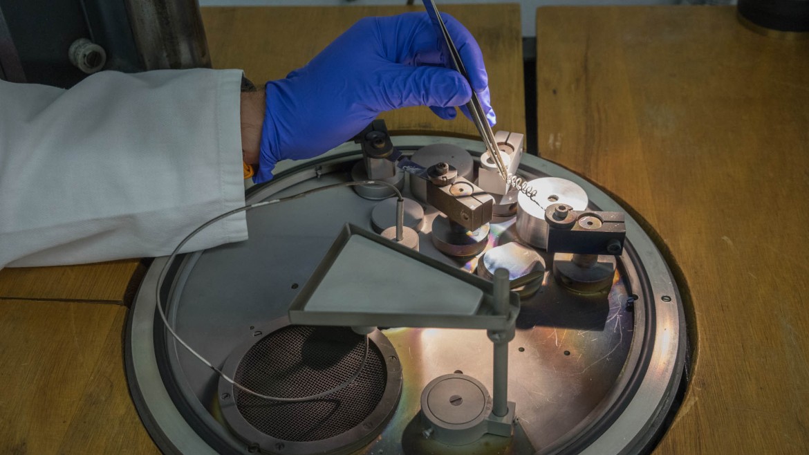
- Production PE-CVD system with spectrometer f. opt. Emission spectroscopy, energy dispersive mass spectrometer
- High-end CVD system with diff. pump and newly developed cooling trap
- E-Beam steaming system
- RF diode sputtering system
- Parallel plate reactor for RIE