Microsystems Technology
Typical semiconductor processes, such as thin film production, optical lithography or etching technology are possible. In addition, work is taking place in the field of printed electronics.
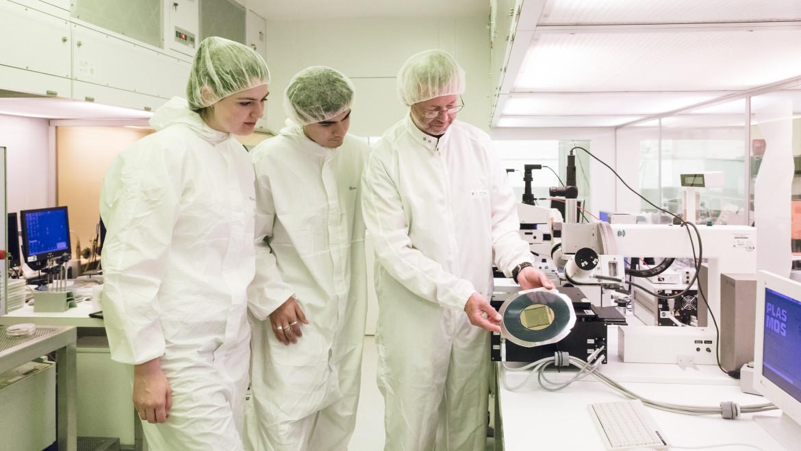
Description
The small 65 m2 clean room is equipped with laminar flow boxes (cleanroom class 10 - 100 at the workstation) and air treatment via ceiling inlets.
Access to the clean room is exclusively via an airlock.
Rooms: D206, D207
Phone: -3630, -3631
- The 65 m2 small cleanroom at the Munich University of Applied Sciences is equipped with laminar flow boxes (cleanroom class 10 - 100 at the workplace) and air treatment via ceiling inlets. Access is via a lock
- In the microsystem technology laboratory there are various commercial plants for the processing of wafers (Si, GaAs, lithium niobate, etc.) in the formats 4'' = 100 mm diameter up to partly 8'' = 200 mm diameter. Many typical semiconductor processes are possible, such as:
- Photolithography (contact, one-sided, on both sides, up to approx. 1 micron)
- Laser lithography (up to 0.7 micron structures)
- Etching technology (wet incl. KOH dry: barrel, parallel plates and RIE)
- Oxidation (moist and dry up to 8'') and diffusion (coming soon)
- CVD (up to 6'') by TEOS, Poly-Si
- Steaming (Al, Cu, Au, Cr, Ni),
- Various measuring techniques are possible:
- Ellipsometer, Spektralellipsometer
- Reflektometrie
- Microscopy with line width measurement
- Confocal microscopy
- White-light interferometry
- Profilometer
- Printed electronics:
- Material printer for insulating, semiconducting and conductive inks from FujiDimatix
- System for photonic sintering of NovaCentrix
- Other:
- Design
- Polishing of 4''-Wafern
- Sawing and cracking of wafers
- Inkjet printing of electronic structures
Topics for project studies or thesis:
- Measuring station extension for characterizing data storage cells
- Printing resistive data memory cells
- Characterization of resistive data storage based on porous silicon
- Printing sensors
Other topics by arrangement.