Solid State Physics
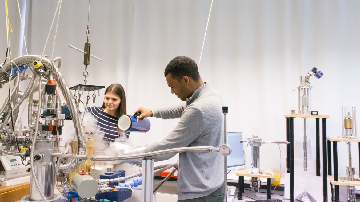
Lab Classes to teach fundamental properties of solids and the ability to apply solid-state physical model systems to concrete applications, including modern semiconductor process technology and sensor technology.

Despription
Investigation of the Structural, Optical and Magnetic / Electrical Properties of Solid Matter. Focus: Material Science Analysis and Characterization of Semiconductor Crystals and Nanostructures. Low temperatures.
Rooms: D208, D209
Phone: -3633, -3664
- FTIR spectrometer (absorption/reflection, 12000 - 100 cm-1, 4 - 300 K)
- Photoluminescence (600 - 1700 nm, 7 - 300 K)
- X-ray diffraction (2-circle goniometer)
- Reverb effect (0 - 4 T, 300 - 400 K)
- Determination of I-U and C-U characteristics
- Capacity transient spectroscopy (DLTS, 77 - 300 K)
- Tunnel microscopy (teaching setup)
- Determination of magnetic sizes
- Surface scanning process
- Sample preparation (sawing, grinding, polishing)
- Infrared absorption measurements (FTIR) on defects in semiconductors (Si, GaAs, etc.)
- Photoluminescence measurements on semiconductors and semiconductor heterostructures
- Time-resolved capacity measurements on metal-semiconductor boundary layer structures
FCM - Freiberger Compound Materials: Oxygen-correlated defects in semi-insulating gallium arsenide
Siltronic: Optical spectroscopy on nitrogen-oxygen complexes in silicon
Wacker Chemie: Infrared optical measurement method for the determination of carbon in polycrystalline silicon
DFG and BMBF projects (focus: defect analysis in semiconductors) with the participation of partners from industry (FCM, Infineon, MEMC, Siltronic, Wacker Chemie).